Optics of Augmented Reality Part 1: Fundamentals
This document is an introduction to the Optics of Augmented Reality. The origin of this text is a pre-read created for Facebook (now Meta) leadership a few years after the acquisition of Oculus, when the scope and scale of AR display efforts began to expand rapidly. The original primary audience was Mark Zuckerberg; the objective was to help build an intuitive grasp of a few key optical principles so that strategic decisions could be more productive. As such, this material is designed for an exceptionally intelligent reader with limited background in optics. This document is Part 1, focusing primarily on foundational concepts and definitions. Part 2 (to be published at a later date) will cover details on specific technologies and the decision frameworks used to select between them within the context of the strategic objectives at the time. To publish this requires me to sanitize the material to avoid proprietary information disclosure.
This is not intended to be an exhaustive treatment. Attempting to cover every nuance would be counterproductive; instead, the focus remains strictly on the specific concepts that dictated strategy at the time, respecting the limited bandwidth of the leadership team. Additionally, for the purposes of this introduction, two fundamental physical components of an AR display system are isolated:
The Display Source: The optoelectronic engine that generates the raw image.
The Optics: The optical system that delivers that image to the user.
While other subsystems—such as eye tracking, adaptive focus (to resolve depth mismatches), and occlusion control (enabling virtual objects to block real-world light)—are also critical, they are intentionally excluded here.
This section introduces the foundational concepts of optics relevant to AR displays, establishing a shared vocabulary for the technical discussions within a broad audience. This is deliberately a targeted conceptual overview rather than an academically rigorous treatment. However, this level of simplification is necessary—a comprehensive treatment of these concepts would require multiple university-level courses.
The goal is to translate complex physics into intuitive mental models directly applicable to evaluating AR engineering approaches. Laying this groundwork requires covering dense material, as it is simply not possible to have a strategic discussion on these topics without addressing the underlying physics. The core objective remains building a functional intuition to empower strategic decision-making rather than a working knowledge for detailed optical design.
The Architecture of an AR Display
Before diving into a detailed glossary, it helps to walk through a typical near-to-eye display architecture—specifically, one that relies on pupil replication.
(Note: In this walkthrough, I deliberately use several technical terms and concepts that will be defined in subsequent sections.)
The Engine
To build an AR display system, we start with a display source to generate the digital image. For this example, we use a miniature, two-dimensional grid of light-emitting diodes—a microLED array. Combining this high-resolution display panel with a series of imaging lenses creates a projector, the core optical engine of our system.
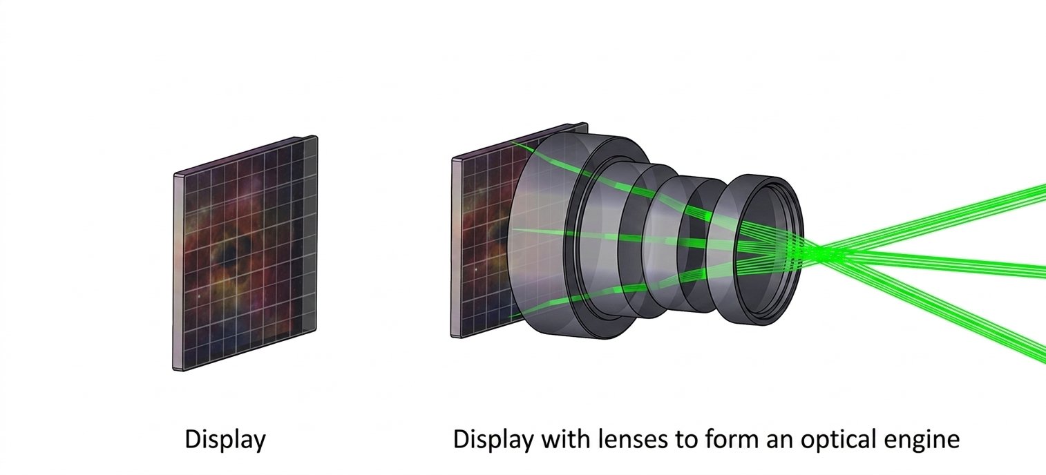
Display source (Right) and the Optical Engine (Left)
Etendue Issues:
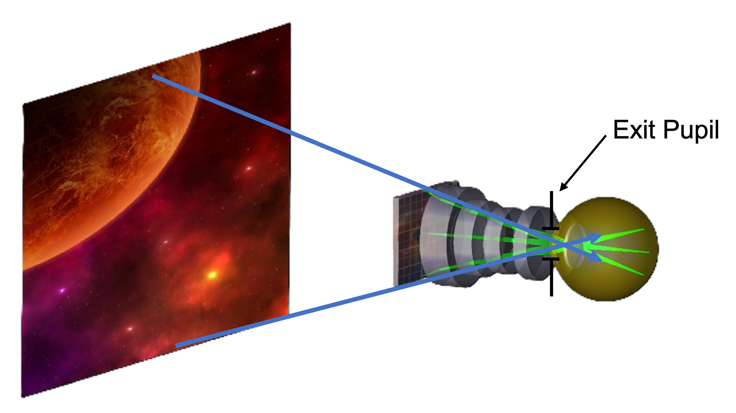
In a simple optical setup, placing your eye directly in front of this projector’s exit window (the exit pupil) allows you to see a magnified version of the digital image floating in space. However, to make this display practical, a traditional projector would need to be relatively large.
This constraint is governed by étendue—the geometric relationship between the Field of View (FOV) and the size of the viewing window. To achieve both a wide FOV and a comfortable viewing window, a standard projector must scale up in physical volume. Furthermore, this bulky projector would have to sit directly in front of your face, blocking your view of the real world and defeating the purpose of AR.
Pupil Replication via Waveguides To shrink the projector while keeping the real world visible, we use pupil replication:
Light Transport: Instead of projecting light directly into the eye, we couple it into a thin, transparent glass plate (a waveguide). Diffraction gratings trap the light inside the plate using total internal reflection. The light propagates inside the glass toward the user’s eye, keeping the optical path out of the primary line of sight.
Replication & Extraction: Out-coupling gratings extract the light toward the user's eye. As the gratings extract the light, they replicate the light bundle into multiple copies.
This combination of redirection and replication allows us to use a compact, temple-mounted projector while presenting a large, comfortable viewing window through a transparent lens approaching an eyeglasses form factor.
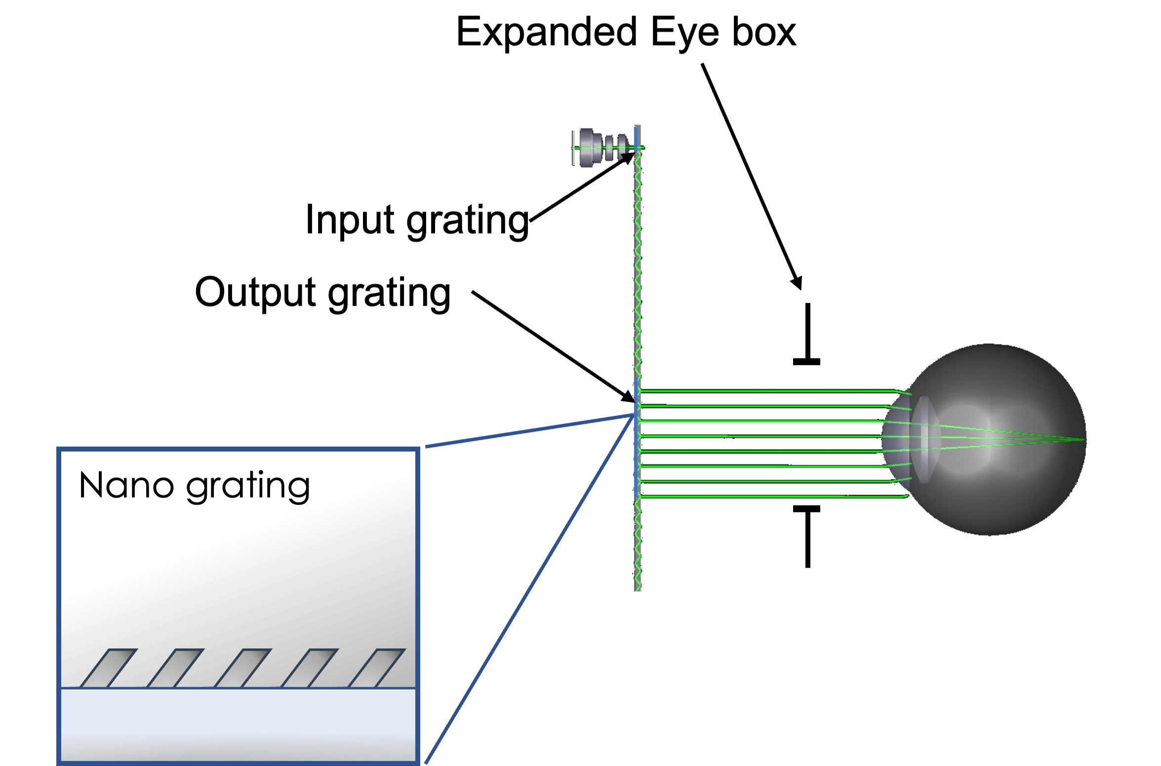
While pupil replication redistributes the available optical phase space over a larger area, total light power is divided across the replicated pupils significantly increasing the brightness and power required from the optical engine.
With this system-level architecture in mind, we can now step back and define the core optical principles that make this replication possible. To keep this digestible, we will divide our definitions into three domains:
Geometrical Optics: Image and Pupil Formation
Physical Optics: Redirect, Trap, and Control Light Fields
Device Physics: Photon Generation
Geometric Optics: Image and Pupil Forming
Virtual Images
The purpose of any optical system is to take a physical object and reproduce its image in another location. In optics, we can talk about images being real images or virtual images. As shown in the diagram below, the type of image formed depends on where our object sits relative to the lens’s focal point.
(Note: The focal plane is the plane perpendicular to the optical axis passing through the focal point, where incoming parallel light rays converge after passing through the lens.)
Real Image (Object beyond focal point): When an object is placed farther from the lens than its focal point (but not at infinity), the light rays converge after passing through the lens. A real image is formed at the point of convergence, meaning you could place a physical screen or sensor there and see a projected reproduction of the object.
Image at Infinity (Object on focal plane): If the object sits exactly on the focal plane, all light rays emerge parallel after passing through the lens. Because parallel rays never intersect, we say the image is formed at optical infinity.
Virtual Image (Object inside focal point): When an object is placed closer to the lens than its focal point, the light rays diverge after passing through the lens. Consequently, no screen placed on the far side of the lens will capture an image because the rays never physically converge. Instead, the rays appear to trace back to an apparent convergence point on the same side of the lens as the object. Because light rays do not actually intersect there, we refer to this as a virtual image.
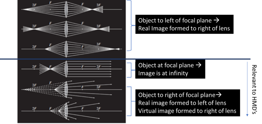
When you look at an object in the real world, every point on that object scatters light outward in a cone of diverging rays. The degree of divergence depends directly on how close the object is to your eye. Your eye collects these diverging rays and focuses them onto the retina to form a real image.
A Head-Mounted Display (HMD)—often referred to as a near-to-eye display (NED)—recreates this physical behavior. The optics of an HMD form light from a microdisplay into parallel or diverging rays that match the angles light would take if it were coming from a physical object placed at a specific distance in space. Because the incoming light enters the pupil with the correct divergence, the eye focuses it onto the retina just as it would for a real object. The key point is that the display system creates similarly diverging light to produce images that are equivalent to real-world scenes, and the images that are created are called virtual images.
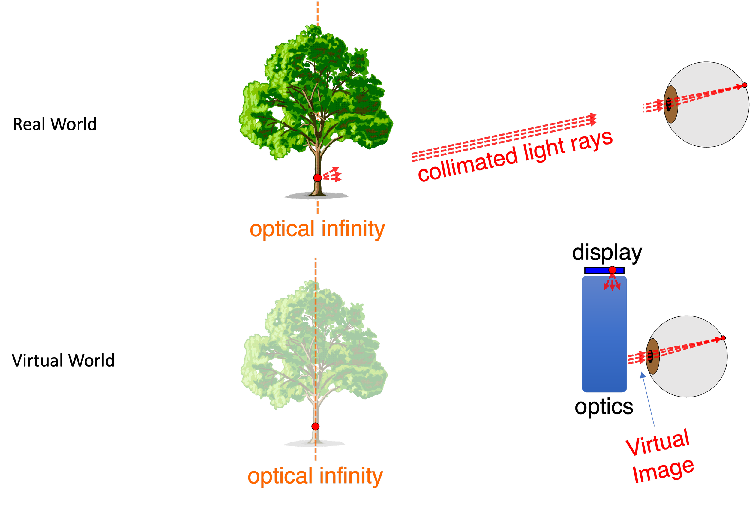
Pupils
An aperture stop is the physical element (like an iris or lens rim) in an optical system that limits how much light can pass through. The "pupils" are the images of this aperture stop as seen from different sides of the optics:
Entrance Pupil: The image of the aperture stop as viewed from the object side (where light enters from the display source).
Exit Pupil: The image of the aperture stop as viewed from the image side (where light exits toward the eye).
In a near-to-eye display, the exit pupil represents the exact physical region where the light rays converge and pass through, establishing where the user places their eye to view the complete virtual image.
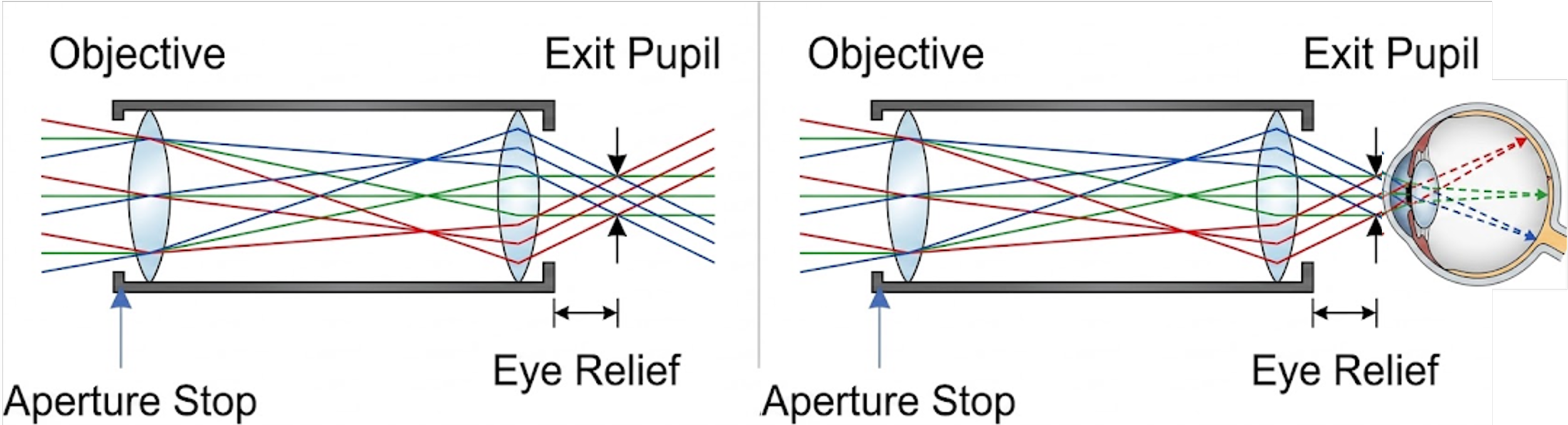
Left - Formation of the exit pupil in an optical system. Right - The user places their eye at the exit pupil in order to view the virtual image.
The eyebox is the three-dimensional volume in space within which the user’s eye can move while still seeing the full, unclipped virtual image. For a user to see the display, the eye's pupil must physically overlap with the system's eyebox.
A familiar example is a pair of binoculars:
7x50 Binoculars: Feature a large 7 mm exit pupil, yielding a eyebox that makes eye alignment easy and forgiving.
7x20 Binoculars: Produce a narrow 3 mm exit pupil, creating a eyebox that requires precise alignment to avoid losing the image.
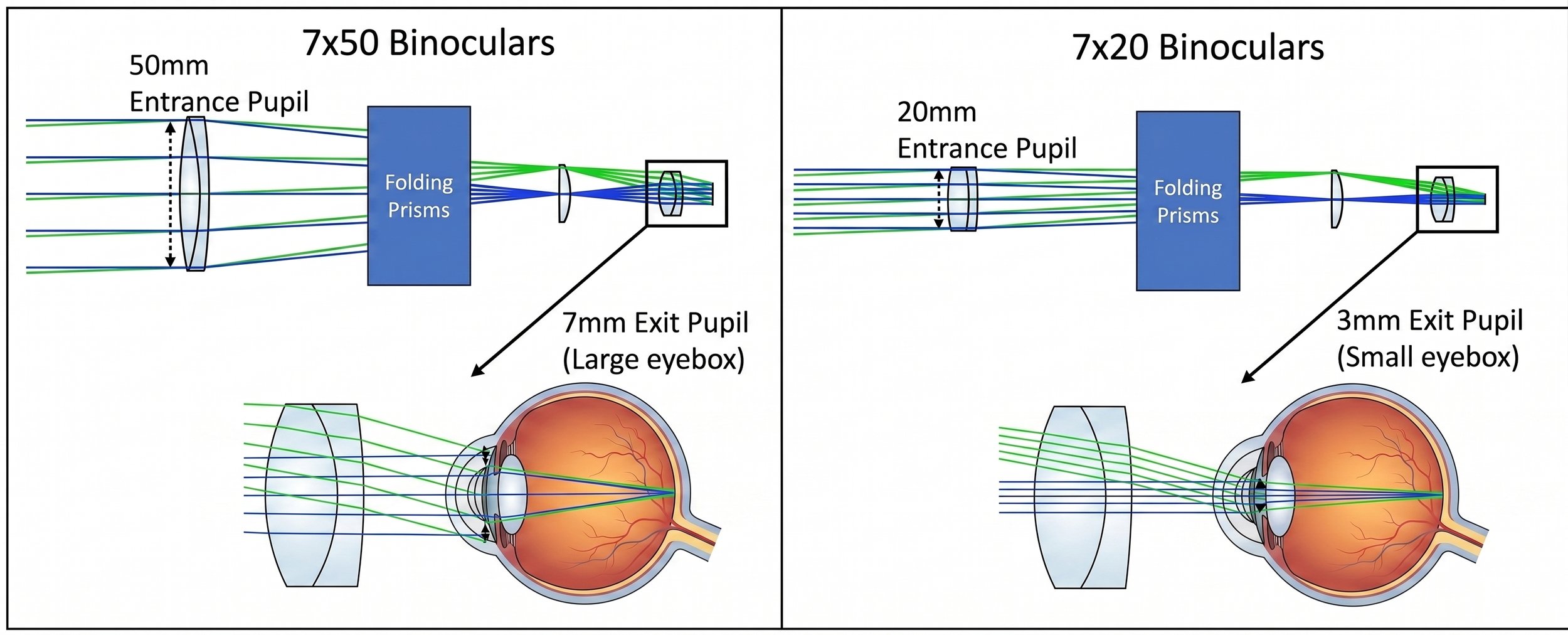
Left - example of binoculars with a large exit pupil allowing easy viewing. Right - example of binoculars with a smaller exit pupil requiring more careful eye alignment.
Achieving a large eyebox is a key consideration in AR architecture. Early compact smart glasses—such as Intel Vaunt or Focals by North—achieved sleek forms by projecting a small, fixed exit pupil directly into the eye. While the virtual image was sharp when looking straight ahead, even minor eye rotations or frame shifts caused the eye's pupil to move out of alignment, resulting in immediate image loss.
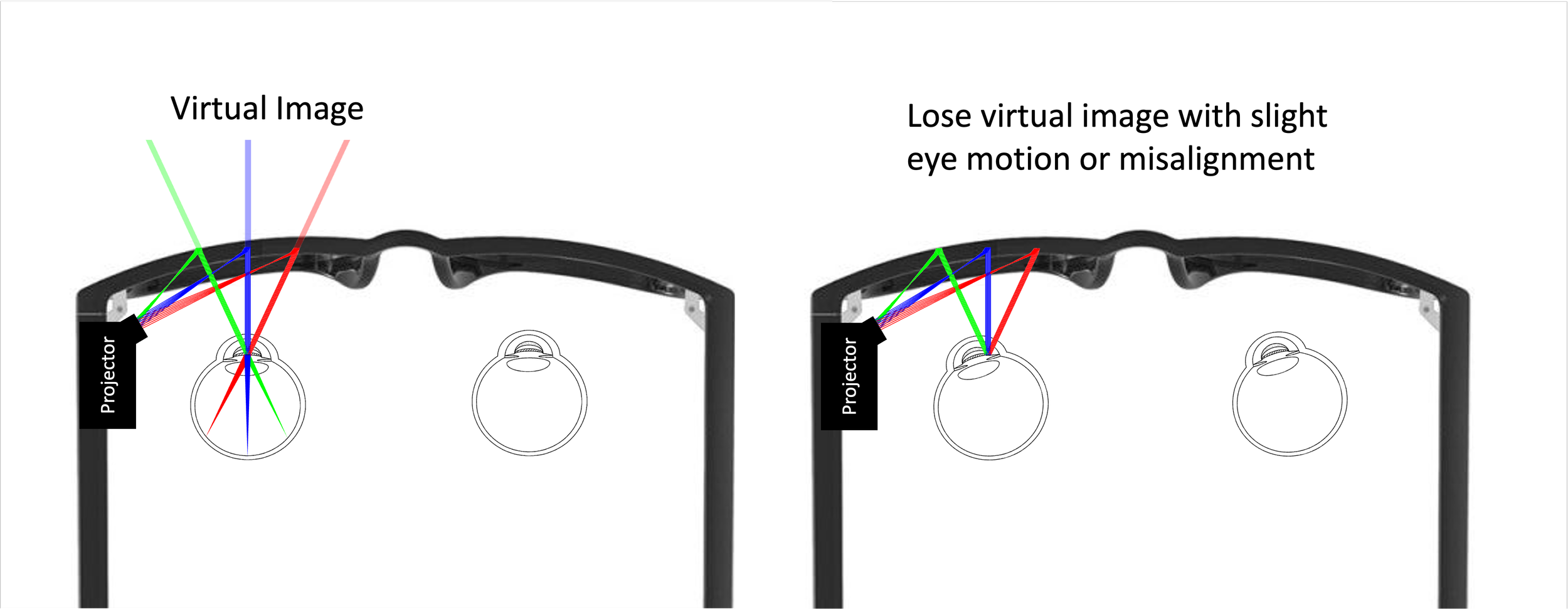
Diagram showing how a small eye is sensitive to small eye movements.
Étendue
Etendue is a fundamental metric of any display or optical system, describing how spread out the light is both in angle spread (for example the field of view or a display emission cone) and area (for example the size of the pupil or the size of the object). Etendue is the product of area times solid angle . The solid angle (measured in units of steradians) is the 3D version of angle (measured in units of radians). Any combination of lossless mirrors and lenses will conserve etendue (see https://what-if.xkcd.com/145/). An AR device produces a small exit pupil because the projector contains a compact microdisplay and compact optics, both of which need to be extremely compact, leading to a smaller etendue. This limits the achievable combination of FOV and exit pupil leading to a choice of large FOV with small exit pupil or large exit pupil with small FOV.
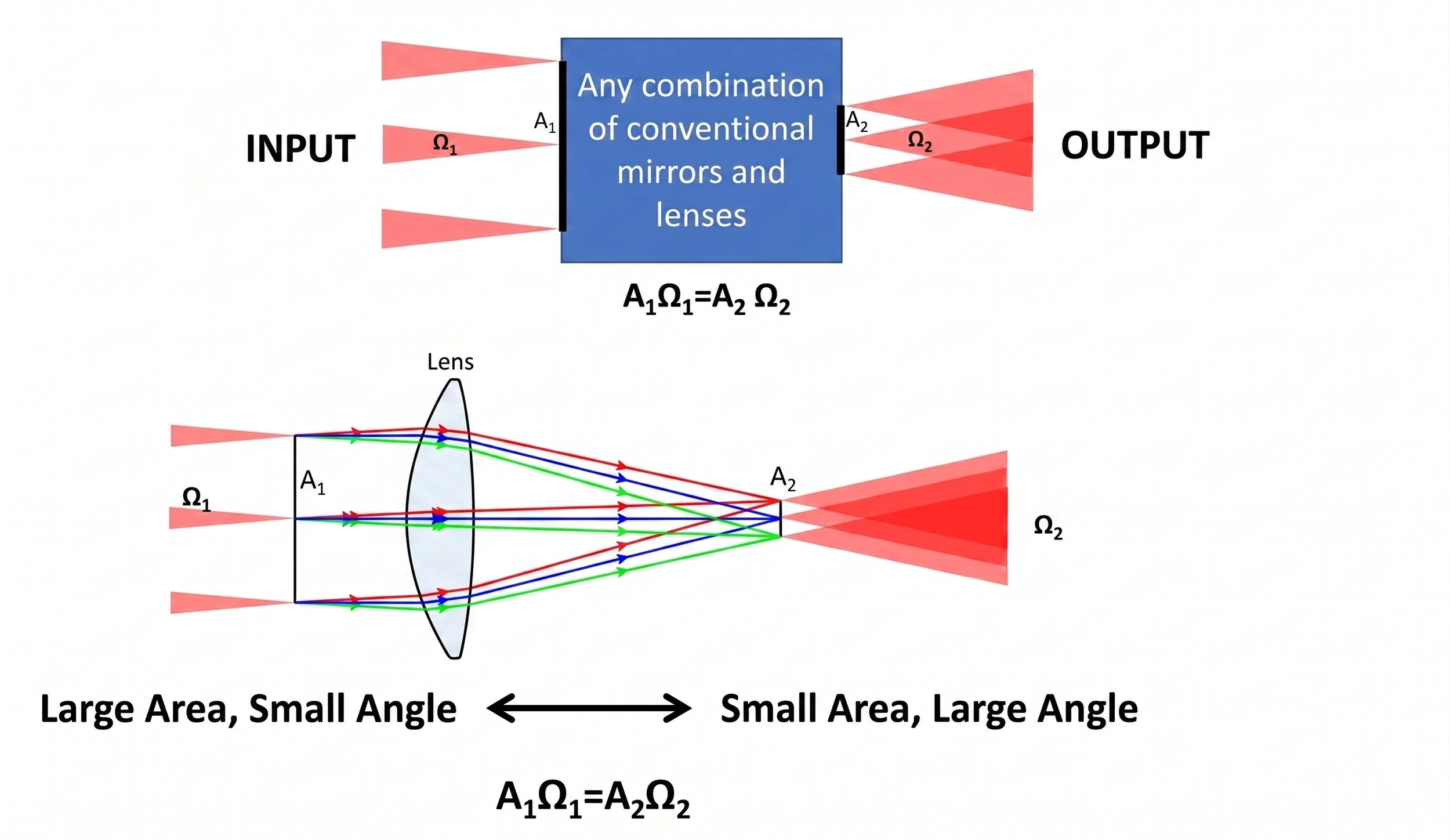
Etendue: The AΩ product is conserved as light propagates through a lossless optical system.
Physical Optics: Redirect, trap, and control light fields
Wave Nature of light
Depending on the problem we are solving, light can be modeled in three ways: as a ray, a wave, or a particle. In display optics, knowing which model to apply comes down to the physical scale of the components involved:
Geometric Optics (Ray Model): We treat light as straight lines (rays) when it propagates through macroscopic components—like traditional lenses and mirrors—that are much larger than the wavelength of light (approximately 500nm).
Physical Optics (Wave Model): When light interacts with sharp edges, micro-structures, or features near or smaller than its wavelength, the ray model breaks down. Directions and energy distributions can no longer be modeled purely through geometry; we must evaluate the wave nature of light by solving Maxwell’s equations (either rigorously or through strategic approximations).
Quantum Optics (Particle/Photon Model): When light interacts at the atomic level—such as photon emission within a microLED or absorption in a sensor—we treat light as discrete energy particles (photons).
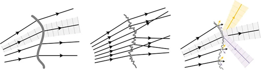
Left – light interacting with a smooth surface can be treated as a ray. Middle – light interacting with complex features that are larger than the wavelength of light can still be treated as a ray. Right – light interacting with a periodic feature or on the order of the wavelength of light must be treated as a wave.
Total Internal Reflection
Total internal reflection (TIR) is the phenomenon which occurs when a propagating wave strikes the boundary between two media at an angle larger than a particular critical angle with respect to the normal to the surface. The angle of light bends at the boundary between two media with different refractive indices; the critical angle is the angle at which the light will bend at 90 degrees from a perpendicular to the boundary (parallel to the surface of the boundary). Since no light can propagate out beyond the boundary past this angle, all the light is totally reflected.
Conceptually, the mechanism is straightforward, but the fields at the boundaries are complex. As the waveguide becomes thin, the description of light propagation inside must be calculated using wave optics. TIR is how light propagates down a waveguide, bouncing losslessly between the surfaces until it encounters a feature that enables it to refract out toward the eye.
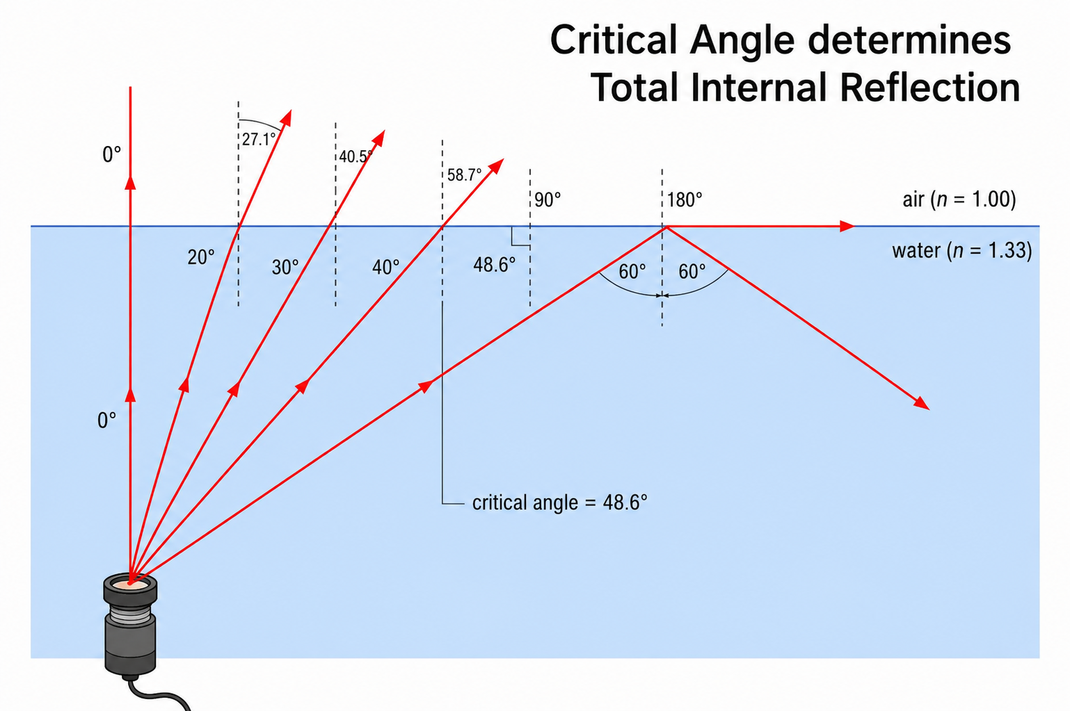
Total internal reflection example for water
Diffraction
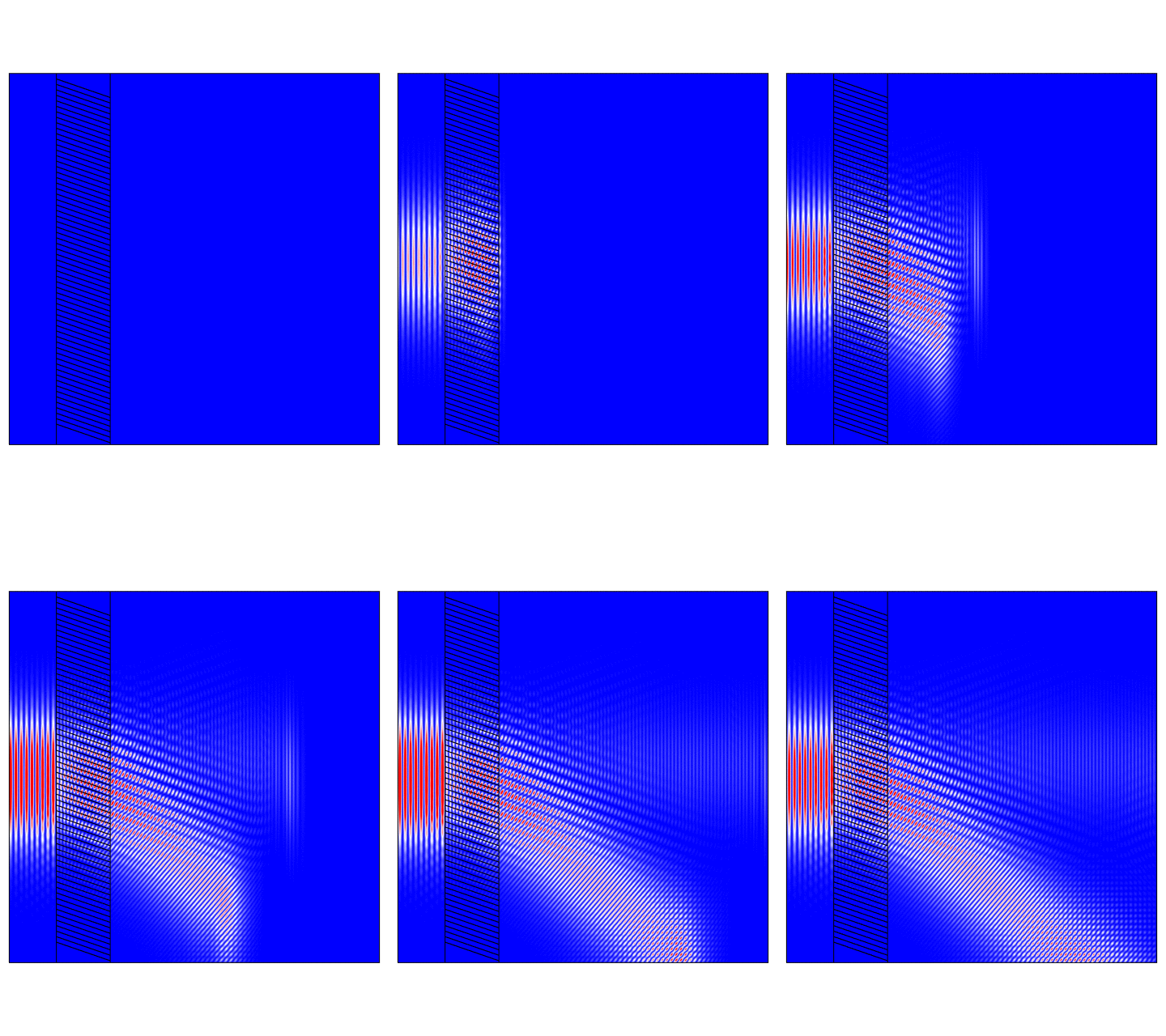
Diffraction happens when light interacts with an edge. The wave nature of light causes it to bend at this boundary, fundamentally setting diffraction apart from refraction. Unlike refraction, which depends on a change in refractive index, the bending in diffraction results from the interference and summation of complex wavelets at the boundary. To accurately calculate the resulting angles and energy distribution, one must solve for all the electromagnetic fields that exist at the edge, sum them up, and determine how much energy propagates in each direction. The figure below illustrates several examples of diffraction and its impact on a single-wavelength plane wave.
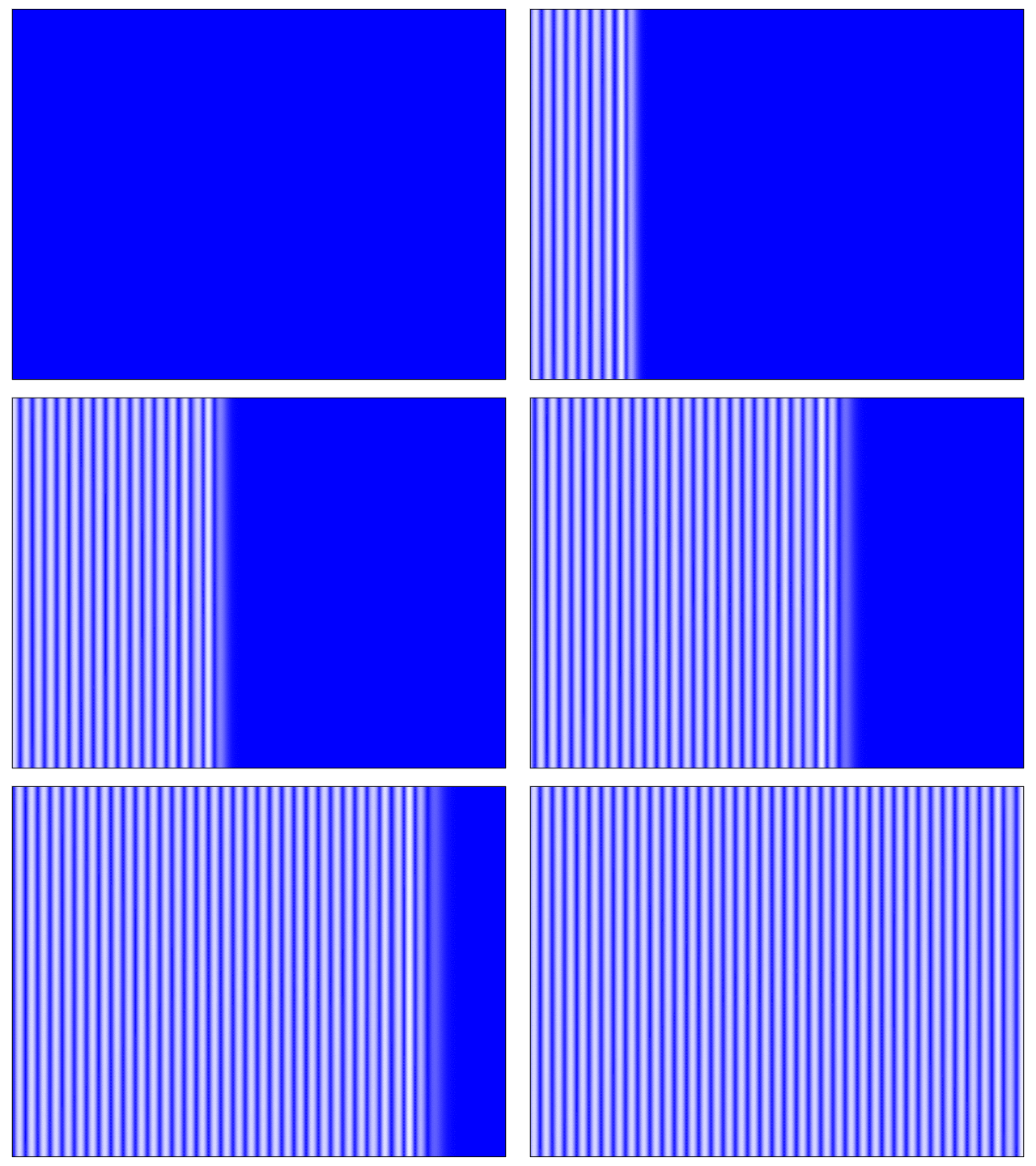
Light propagating with no aperture
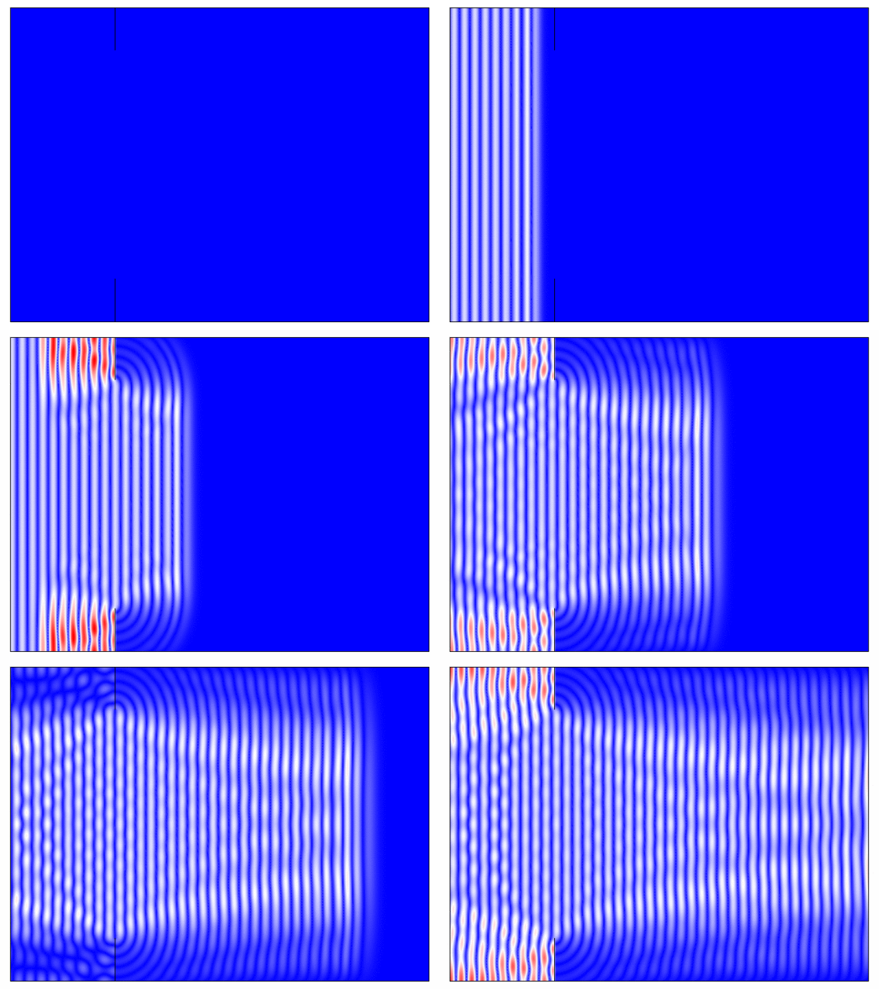
Light propagating with large aperture
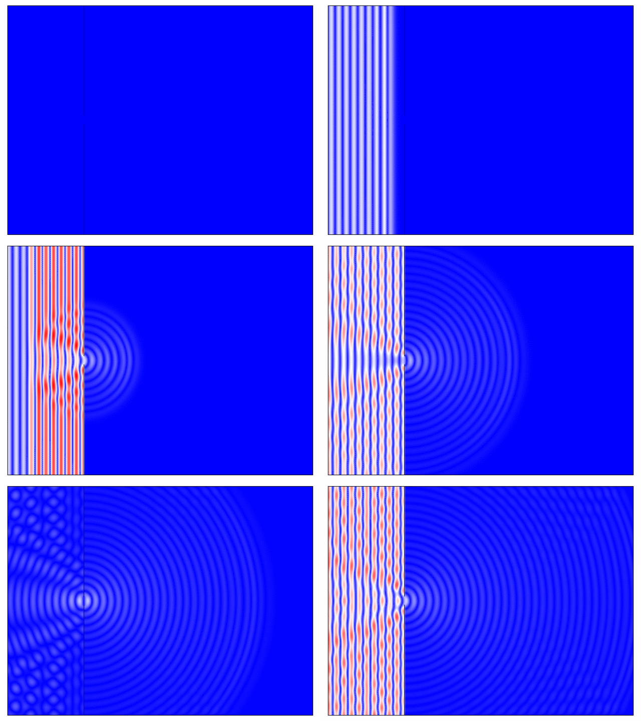
Light propagating with small aperture
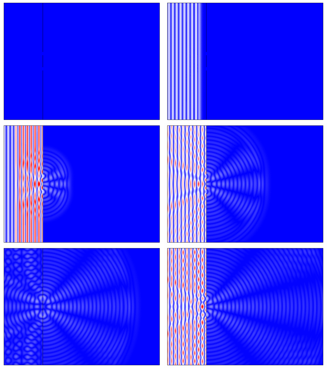
Light propagating with dual aperture
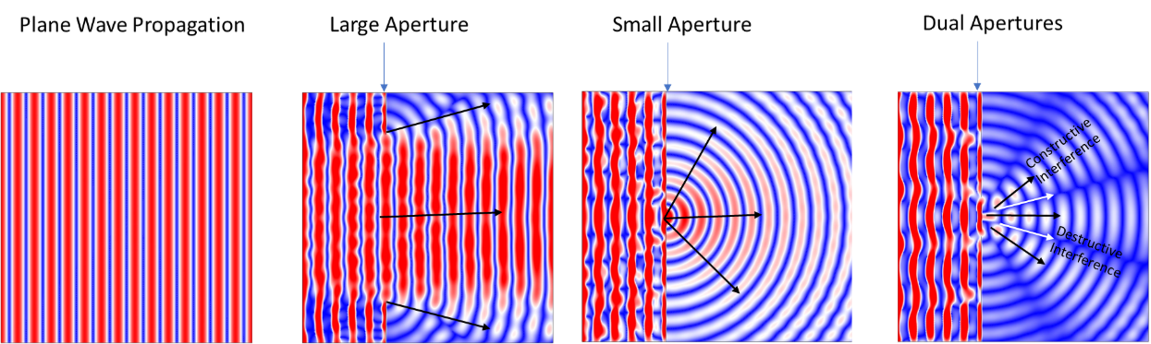
Still images showing the response of the light after interacting with the apertures.
A diffraction grating is a periodic modulation that creates a multitude of edges, using either apertures (amplitude modulation by altering boundary geometry) or materials (phase modulation by altering material properties). These structures are designed to set up complex fields that direct optical energy in very specific ways. The smaller the spacing between these structures, the greater the angle at which the light will diffract. In our context, we rely on phase modulation, which can be achieved by using two transparent glass-like materials or a single material interfaced with air.
Both the angle and the amount of energy directed by a diffraction grating depend strongly on wavelength. Because gratings rely on the constructive and destructive interference of complex electromagnetic fields, the nature of these interactions changes directly with the wavelength of the light involved.
The diagram below illustrates the progression from dual apertures to a high-density aperture array, and finally to a multi-aperture interaction with white light. When the number of apertures is very large, the summation of the electromagnetic fields results in light propagating strictly along distinct, allowable angles. These allowable paths are called diffraction orders, with the zero order representing the angle where light passes straight through without any change in direction.
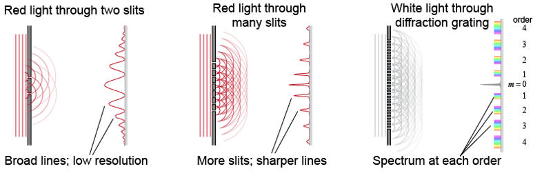
Progression of diffraction of light moving from a single wavelength double slit to many slits to many slits with white light.
Typically, the diffraction process will have two regimes. These are called the Raman Nath regime and the Bragg regime. Raman Nath type gratings have many diffraction orders and work over very large angle and wavelength ranges. The Bragg regime will only diffract into 1 order so light will either go into that order or will continue to propagate, and they typically work over a narrow angle and wavelength range. We refer to this wavelength and angle as the so-called Bragg Condition. The type of diffraction grating created depends on the relationship between the index modulation level (that is, the difference in refraction index between the two materials) of the material and the size of the features. The higher the index difference between two materials or the larger the features, the more likely the diffraction will be in the Raman Nath regime.
A grating is the term used for the modulation of materials or apertures that creates the diffraction process. In the figure below I show two examples. A surface relief grating is a grating where features are created on the surface to create the diffraction process. Surface relief gratings (SRG) are typically Raman Nath type gratings because the grating has one material and air so the index difference is very large. A designer would work to create a specific structure to control the amount of energy going to a given angle over a given wavelength range. The rest of the energy will either continue to propagate or go to other diffraction angles.
Bragg gratings are gratings that create Bragg diffraction at wavelengths and angles that are close to the Bragg Condition. These are typically created by writing an index modulation into a photorefractive material in which you can change the index by exposure to different light sources. Holograms are a special case of Bragg Diffraction. Bragg gratings have the advantage that they are very efficient in directing light but generally work only over a limited angle and wavelength range.
Bragg Diffraction from a volume Bragg grating (VBG)

Raman Nath diffraction through a surface relief grating (SRG)
Coherence
Coherence is a property of a light field that measures the ability of the light to constructively or destructively interfere with itself—essentially representing the degree of order within that light field.
One primary form is temporal coherence, which measures order over time. It is characterized by coherence length, defined as the path distance over which light can maintain a fixed phase relationship and interfere with itself. If you split a light beam into two paths and then recombine them, the coherence length is the maximum path length difference over which those two beams will produce interference. Lasers possess exceptionally high temporal coherence, allowing them to interfere even when there is a significant path length difference between the split beams. The practical implication in display optics is that laser sources can introduce unwanted intensity modulations, manifesting as speckle or non-uniformities that degrade image quality. LEDs have a much shorter coherence length which can mostly eliminate interference artifacts, though speckle and non-uniformity effects can still emerge in highly precise optical systems.
Another form is spatial coherence, which measures spatial order across the phase front. When light originates from an exceptionally small or point-like source, it exhibits high spatial coherence because that point can be almost perfectly reconstructed by an optical system. As the physical size of the source grows, the ability to sharply reconstruct any specific point degrades due to mutual interference between adjacent emitting points. Because each point on an extended source generates a slightly shifted interference pattern, their summation deviates from the ideal point spread function, leading to reduced resolution and lower contrast in high-resolution displays.
The figure below outlines both temporal (left) and spatial (right) coherence.
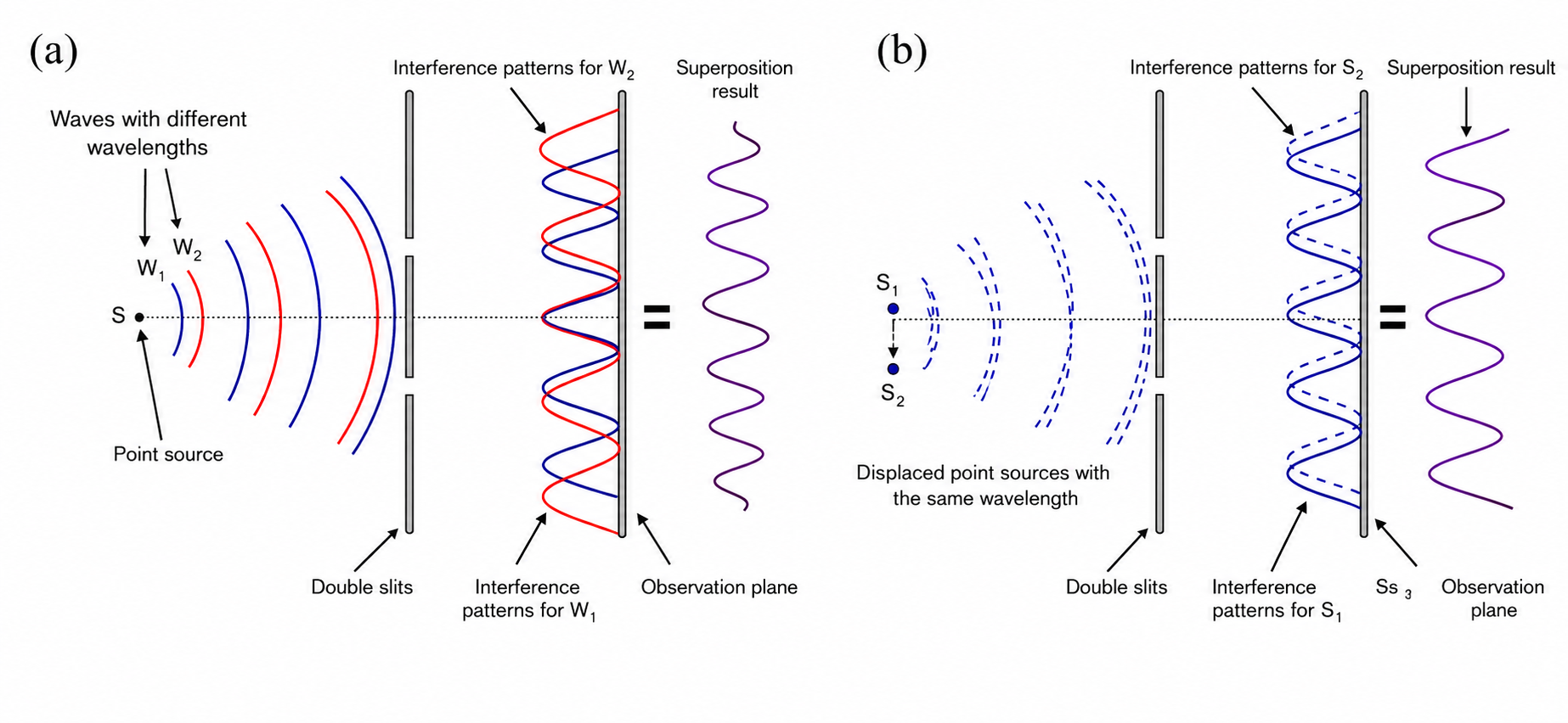
The left side (temporal coherence) shows a single point source emits light containing multiple wavelengths (W1 and W2). At the center of the observation plane, light rays traveling from the double slits cover equal path lengths, allowing the interference peaks of all wavelengths to align perfectly. However, moving outward from the center causes path length differences to accumulate at varying rates depending on the wavelength. As a result, the individual interference sub-patterns shift out of alignment with one another, causing the overall modulation contrast to progressively decrease toward the edges while remaining sharp in the middle.
The right side (spatial coherence) shows two spatially displaced point sources (S1 and S2) emit light of the exact same wavelength. Because source S2 is physically shifted relative to S1, it generates an interference pattern that is uniformly displaced across the entire observation plane. Rather than degrading from the center outward, these two shifted fringe patterns overlap evenly everywhere. Consequently, the presence of multiple spatially separated sources reduces the overall modulation contrast uniformly across the entire field of view.
Polarization
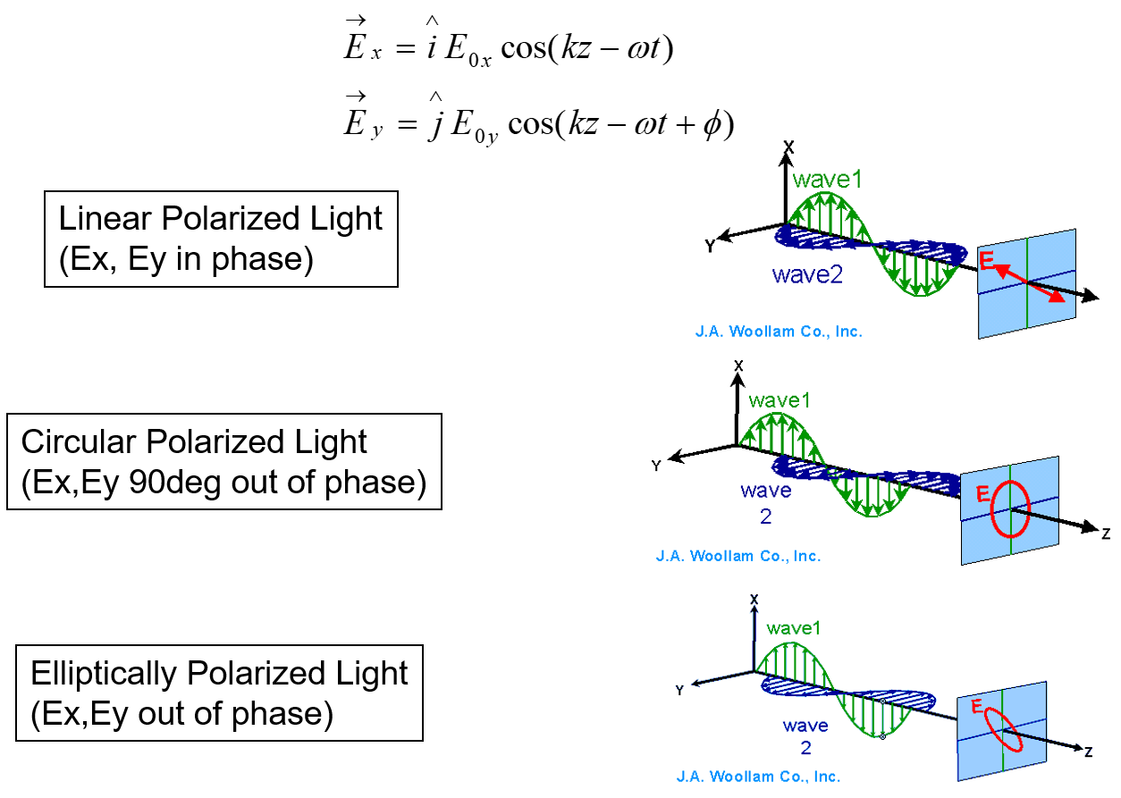
Polarization describes the orientation of the electric field as light propagates. Light travels along a specific direction, and its polarization is a measure of the field's orientation in the plane perpendicular to that path. A light field can be polarized or unpolarized (or depolarized)—where polarized means the electric field vectors across all rays maintain a structured alignment, and unpolarized means the polarization states are randomly disordered.
For polarized light, the most general state is elliptical polarization, where the electric field vector traces an ellipse as the wave travels forward. Linear polarization and circular polarization represent special cases of this general state. Managing polarization is critical in near-to-eye display architectures, as the performance and efficiency of most microdisplay sources and optical components are strongly polarization dependent.
In augmented reality architectures, polarization and coherence are critical, system-wide considerations. Different display sources and waveguide combiner technologies exhibit highly divergent optical behaviors based on the unique pairing of these two wave properties. Consequently, a primary challenge in display system engineering lies in precisely matching the polarization and coherence characteristics across these distinct subsystems.
While conceptually straightforward, this architectural optimization can be exceptionally difficult due to the complexity of modeling these multi-variable wave interactions. Furthermore, moving beyond theoretical simulation to experimental validation and mass manufacturing introduces severe real-world hurdles. Because polarization and coherence are sensitive to subtle physical variations, material properties, fabrication tolerances, and mechanical stresses can cause significant performance deviations from the idealized design.
Device Physics: Photon Generation
This next section introduces some basic concepts of device physics which are important in the design of AR display systems. At the heart of much of device physics is a p-n junction—the microscopic boundary formed when two differently treated semiconductor materials are brought into contact: an "n-type" material with an abundance of mobile electrons, and a "p-type" material containing vacant, lower-energy spaces (known as "holes") for those electrons to occupy.
When we apply an electrical current, we inject electrons across this junction, forcing them into a high-energy, "excited" state. Because physical systems naturally seek stability, these excited electrons eventually drop back down to fill the vacant, lower-energy states. To balance this drop in energy, the electron must shed its excess energy, doing so by releasing a discrete packet of light—a photon. The exact size of this energy drop (material bandgap) is what dictates the specific color and wavelength of the light generated.
Display sources utilized in augmented reality architectures generally fall into two categories: Light-Emitting Diodes (LEDs) or semiconductor Lasers. While their operational and performance profiles differ dramatically, both devices rely on semiconductor p-n junctions to achieve population inversion—a state where electrons are driven into an excited, high-energy level—to enable the subsequent emission of photons.
Spontaneous and Stimulated Emission
When an excited electron transitions back to a lower energy level of its own accord, it releases its excess energy by emitting a photon. Because this drop occurs independently and randomly, the resulting photon wavelength, polarization, and direction are probabilistic—a quantum process known as spontaneous emission. LED architectures are engineered to maximize these spontaneous transitions, which naturally produces light that radiates over a wide, unpolarized angular range with very low temporal and spatial coherence.
Conversely, stimulated emission occurs when an incoming photon of a specific wavelength interacts with an already excited electron. This interaction stimulates the electron to drop to its lower energy state, releasing a new photon that is a precise clone of the first—sharing the exact same wavelength, phase, polarization, and direction of travel. When a p-n junction operating under population inversion is exposed to a dense supply of these synchronized photons, it triggers a cascading chain reaction of stimulated emissions. This collective, in-phase behavior is what yields the exceptionally high spatial and temporal coherence that serves as the defining physical signature of laser light.
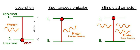
Left: Absorption of a photon causes an electron to move to a higher energy level. Middle: Electron drops to a lower energy level causing a spontaneous emission of a photon. Right: A photon drops to a lower energy level stimulated by existing photons causing stimulated emission
LED’s and Lasers
An LED is fabricated from a semiconductor p-n junction and emits light when an electrical current flows through it. As electrons cross from the n-region to recombine with holes in the p-region, they undergo energy state transitions that, in specific materials, release photons. This radiative recombination occurs efficiently only in direct bandgap materials, such as gallium arsenide (GaAs) and gallium nitride (GaN), where the material chemistry and atomic doping dictate the specific wavelength of the emitted light. In contrast, indirect bandgap materials, such as silicon and germanium, cannot easily emit light because their electronic transitions require a change in momentum; as a result, their recombination process is non-radiative, releasing energy as heat.
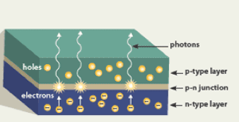
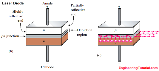
Diagram of LED (Left) and Laser (Right)
To evaluate display performance, we characterize LED efficiency using two critical metrics:
Internal Quantum Efficiency (IQE): The ratio of injected electrons that successfully convert into photons within the active region of the semiconductor crystal.
External Quantum Efficiency (EQE): The ratio of those generated photons that actually escape the physical boundaries of the semiconductor package to become usable light. Both IQE and EQE are vital drivers of the display's overall efficiency, directly dictating headset power consumption and thermal management.
A semiconductor laser shares the same underlying p-n junction architecture as an LED, but introduces an essential structural addition: an optical resonant cavity. This cavity guides and traps the light, forcing generated photons to bounce back and forth through the active p-n junction multiple times. Each pass triggers a cascade of stimulated emissions, cloning and multiplying the synchronized photons in-phase. A small, highly controlled fraction of this amplified light is permitted to escape through a partially reflective boundary at one edge of the cavity.
This resonant feedback loop results in an exceptionally narrow emission angle, a precise spectral wavelength, and highly efficient electron-to-photon conversion. However, because this amplification mechanism produces light with an extremely long coherence length, utilizing lasers as an AR display source introduces significant system-level challenges—such as visible speckle and brightness non-uniformities—that must be mitigated downstream in the optics.
Issues with LED’s
(The next few paragraphs discuss issues in LED’s. I included this because the LED efficiency was a major concern when preparing this writeup to leadership. There are many issues in both LED’s and Lasers that need addressing but I included this to clarify terms related to microLED’s)
A major bottleneck in high-brightness LED design is a phenomenon known as efficiency droop, where the device's internal quantum efficiency (IQE) rapidly declines once the operating current exceeds a certain threshold. As illustrated in the figure below, this drop-off represents a severe challenge when driving displays to the ultra-high luminance levels required to overcome bright, outdoor ambient environments in augmented reality systems.
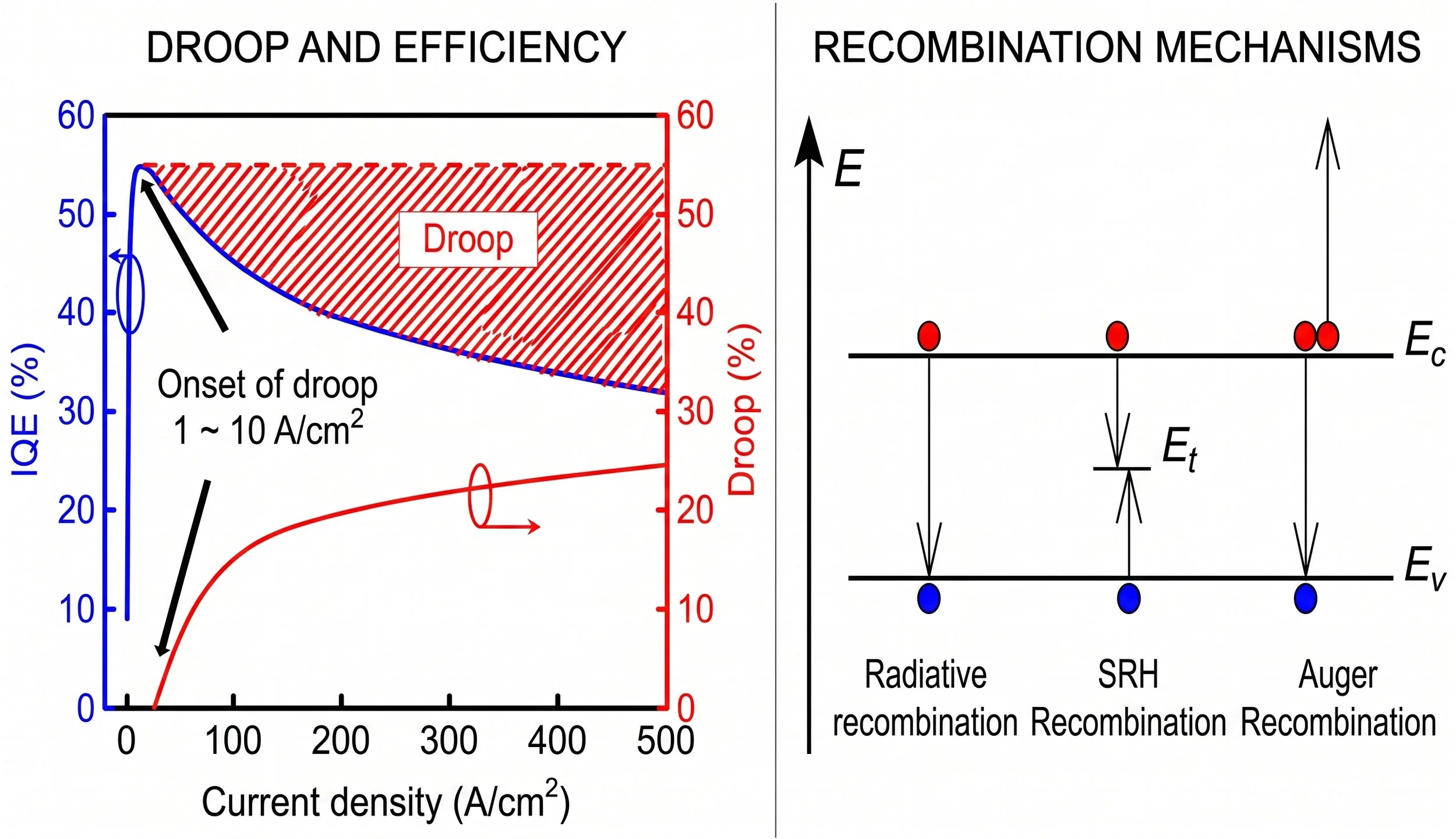
Fundamentally, an LED’s efficiency is governed by a dynamic competition between productive radiative recombination (which generates photons) and various unwanted non-radiative recombination channels (which convert electrical energy into heat).
At high operating currents, one important contributor to efficiency loss is Auger recombination. Auger recombination is a non-radiative process involving three charge carriers. In a direct Auger transition, an electron and a hole recombine, but instead of emitting a useful photon, they transfer their transition energy directly to a third carrier—either exciting an electron higher into the conduction band or pushing a hole deeper into the valence band.
Because this process involves three carriers, its rate increases very rapidly with carrier density—approximately with the cube of carrier density in the simplest model. At sufficiently high current densities, Auger recombination can therefore become a significant loss mechanism, contributing to the characteristic “droop” in efficiency.
Conversely, at lower current densities, the primary non-radiative loss channel is Shockley-Read-Hall (SRH) recombination, commonly referred to as trap-assisted recombination. Unlike Auger recombination, SRH is heavily dependent on the intrinsic quality and crystal purity of the semiconductor material. In this process, an electron falling toward the valence band becomes captured by an intermediate energy state (or "trap") situated within the material's bandgap, which is typically caused by a localized crystal defect, dislocation, or impurity. This trap prevents the electron from completing a clean, direct band-to-band transition, forcing it to release its energy as lattice vibrations (heat) rather than light. Mitigating SRH losses is therefore directly tied to optimizing material growth and fabrication processes to minimize structural defects.
Conclusion of Part 1
Applying these foundational principles of optical and device physics back to our initial near-to-eye display example brings the entire system architecture into clear focus. By walking through the optical path, we can see precisely how device physics, geometrical optics, and physical optics interact to form a functional AR display:
The Display Source (Device Physics): Photon generation begins at the display source. In our microLED array example, current injected across a p-n junction drives spontaneous emission, converting electrical energy into an unpolarized, incoherent cone of light. Managing display efficiency requires balancing carrier dynamics—mitigating defect-driven SRH recombination at lower current densities and Auger recombination at high current densities to combat efficiency droop.
Alternatively, we could have selected a laser-based architecture which relies on stimulated emission within a resonant cavity, producing light with high temporal and spatial coherence, but we know that this can introduce unwanted interference artifacts as it travels through the system.
Image Formation (Geometrical Optics): The microdisplay is paired with optics to form a virtual image. For a practical system, the exit pupil (or eyebox) must be large enough for the user to comfortably view the virtual image. However, a compact projector has a small aperture, thus conservation of étendue forces a direct trade-off: expanding the field of view inevitably shrinks the size of the exit pupil, and vice versa. To increase both, one would need to increase the size of the system, making it incompatible with the size and weight required for an eyeglass form factor.
Guiding and Extracting Wavefronts (Physical Optics): To address the étendue constraint without increasing the system size, light is coupled (using a diffraction grating) into a thin glass waveguide. The coupled light now exceeds the critical angle, allowing the light to propagate within the substrate via total internal reflection. Diffraction gratings—such as surface relief gratings operating in the Raman-Nath regime or volume Bragg gratings operating under strict Bragg conditions—redirect the light and slice the propagating wavefront into multiple copies. This out-coupling process replicates the exit pupil over a larger spatial area, creating a large eyebox for the user.
Ultimately, performance of the system depends on many factors, but polarization and coherence are key considerations not only in the development of the architecture and the design of the components; managing these is key to the realized performance experimentally and ultimately in mass production.